The development of instrumentation for measurements in the field of nanometrology
Special devices for microscopy
As follows from the general description of morphology measurements on the nano and microscale,
it is necessary to develop dedicated devices for measurements with very small uncertainty. In our department, we are developing our own devices even though
we are equipped with several commercial microscopes. The devices that we are developing should primarily cover measurements that are not possible with commercial
devices for their limited accuracy or range.
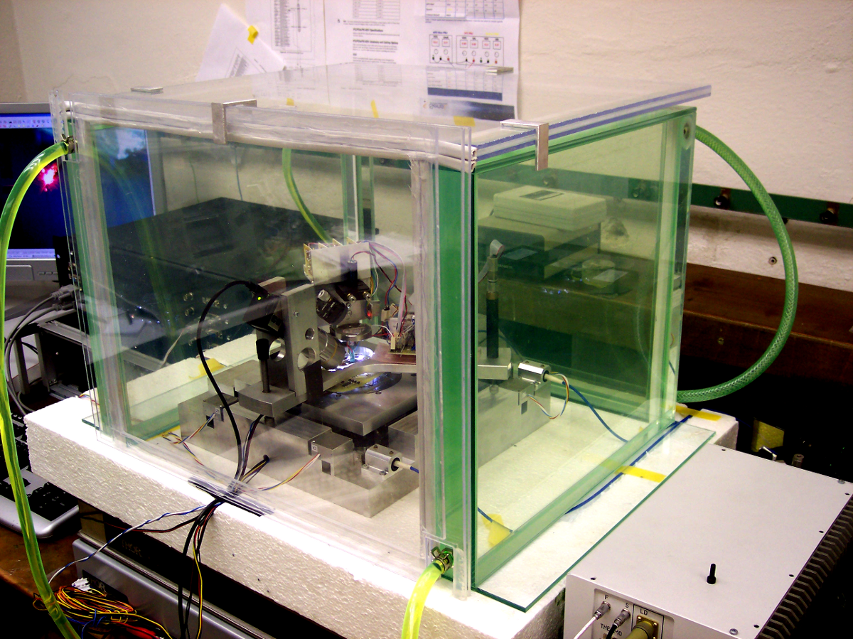
A device being developed as a national standard of length and shape in the field of nanometrology should be the state of the art device.
It was developed in collaboration with the Institute of Scientific Instruments ASCR in years 2007-2011 as a result of a grant cooperation in
"Nanotechnology for a Society" program funded by the Grant Agency of the Czech Republic and it is characterized by its six axis laser interferometric system
which is the basis for measurements with very small uncertainty.
|
The interferometric system developed by the Institute of Scientific Instruments ASCR uses a stabilized Nd:YAG laser,
which is led by the fiber optics to six interferometric units placed around a Physik Instrumente positioning table. Above the table there is a simple AFM head
acting as a passive force sensor between the probe and surface.
The device was involved in a international laboratory comparison in 2008 and nowadays it can be utilized to the most accurate measurements
which can be offered by CMI to the customers in the field of nanometrology. Detailed information on the construction of the device can be found in scientific papers, e.g. [1].
The device is not used as a service to the public only, but it is used also for research activities in the field of uncertainty in SPM measurements.
In particular, it is used in the analysis of the influence of uncertainties of the positioning table on the acquired data [2].
|
 |
| Metrology SPM prototype |
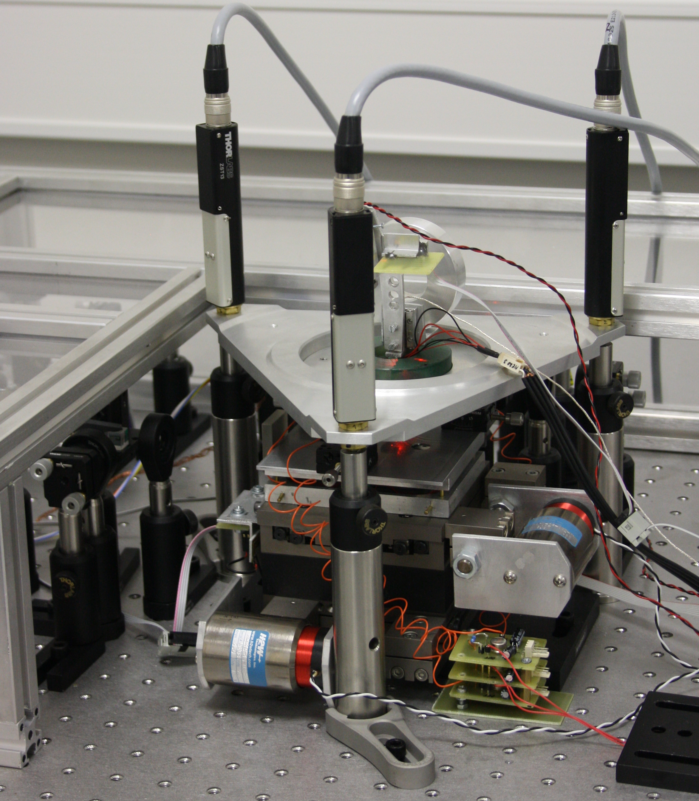
In many cases we don't need to measure with such a small uncertainty but on really large areas (from the point of view of microscopic methods).
For such type of measurements we constructed a long range microscope which is conceptually different from any commercial microscope.
Instead of commonly used piezoelectric actuators this device uses a system based on electromagnets, i.e. coils in combination with permanent
magnets (a voice coil). The coils are in feedback with an interferometric position sensor; the feedback is realized by a cheap microprocessor ATxmega128A1
where a fuzzy logic steering is implemented. Since the microscope table constructed from commercial ball bearing stages is not affected by any force (except of a small
friction force) we are able to set the position of the system in the range of several centimeters with an uncertainty of about 15 nm even though only 12 bit DA converters
are used for the coils feeding. The head of the microscope in this case does not consist of the force sensor only but also of a microactuator in the z axis.
A detailed description of the device can be found in [3].
 |
 |
| Long range microscope |
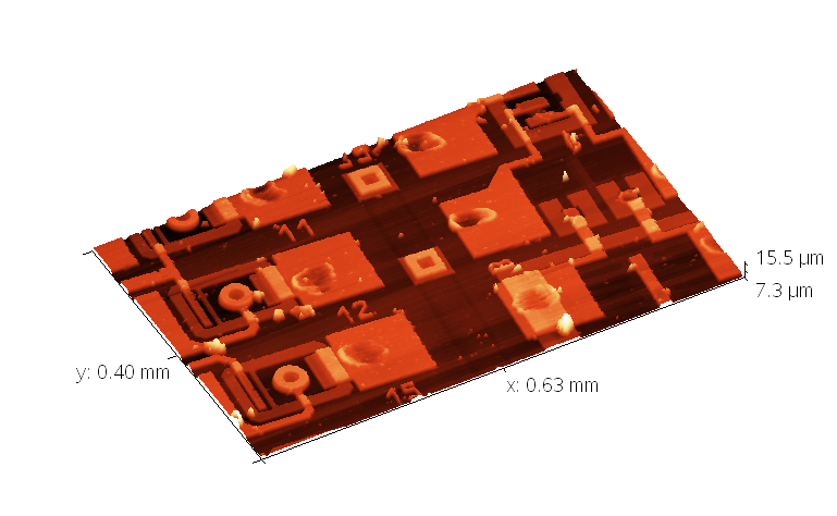
Result of a morphology measurement of a microelectronic component. |
Also other devices were built in similar manner in our department, see e.g. [4].
The construction of own devices has the advantage of the ability to carry out research in the field of AFM data acquisition.
For example during the acquisition with irregular sampling which is the way of how to perform
AFM measurements on large areas with high resolution we are still able to create data files with adequate size and in adequate time [5].
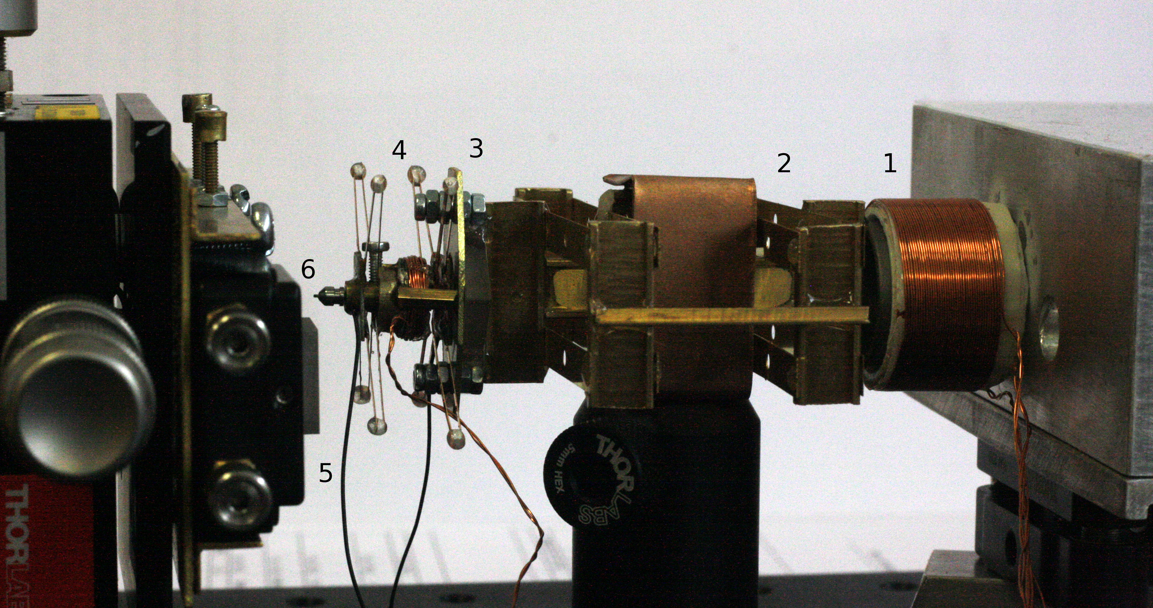
Nanoindentation and microindentation
In the field of a mechanical testing we are also trying to develop our own devices. One of the first tool was an interferometric system for
calibration of commercial nanoindentor providing the traceability to the primary mass standard (platinum kilogram - mass comparator - nanoindentor) and to
the primary length standards (stabilized laser - nanoindentor) [6].
|
Nowadays we are working on the construction of our own nano/microindentor. Although it is expected to have worse resolution and
a smaller range of applicable loads compared to commercial devices, it should provide much simpler traceability chain and thanks to that also smaller uncertainties
in force and displacement.
This research brings us know how in the field of experiment control in the nanoindentation domain which is useful for an uncertainty determination.
|
 |
| CMI's devices for micro and nanoindentation |
[1]J. Lazar, P. Klapetek, O. Číp, M. Čížek, M. Šerý, Local probe microscopy with interferometric monitoring
of the stage nanopositioning, Meas. Sci. Technol., 20, 084007
[2]Petr Klapetek, David Nečas, A. Campbellová, A. Yacoot, L. Koenders, Methods for determining and processing 3D errors and uncertainties for AFM data analysis,
Meas. Sci. Technol., 22, 25501, 2011
[3]P. Klapetek, M. Valtr, M. Matula, A long-range scanning probe microscope for automotive reflector optical quality inspection,
Meas. Sci. Technol. 22 094011
[4]P. Klapetek, M. Valtr, V. Duchoň, J. Sobota, Voice coil-based scanning probe microscopy, Nanoscale Res Lett. 2012; 7(1): 332.
[5]P. Klapetek, M. Valtr, J. Buršík, Non-equidistant scanning approach for millimetre-sized SPM measurements,
Nanoscale research letters. 01/2012; 7:213
[6]A. Campbellová, M. Valtr, J. Zůda, P. Klapetek, Traceable measurements of small forces and local mechanical properties,
Measurement Science and Technology. 08/2011; 22(9):094007
|

