Electric and Magnetic properties
The analysis of a local electric conductivity and the distribution of an electrostatic field is another task related to
the current boom in microelectronics, optoelectronics or solar cell industry. Considering the fact that the local electric resistance in
the microstructure where the electric current is flowing is directly connected to the heat being generated (which represents not only the loses
but also causes a deterioration of the functionality), we are trying to develop methods for electric phenomena mapping with a highest
possible resolution.
Also here is the main tool the scannig probe microscopy - in this case it uses a conductive probe biased by a voltage or we
can measure a voltage generated on it. By a closing of a electric circuit between the probe and the sample we can measure the current and
hence the electric conductivity. If the probe is moved in a close proximity to the surface but not touching it we can evaluate the electrostatic
forces acting between the probe and the surface and it can be used afterwards either for eletrostatic field mapping (Electric Force Microscopy - EFM) or for the measurement of a contact potential between the probe and the sample (this technique is called the Kelvin
Probe Force Microscopy - KPFM).
Although the current or the voltage can be measured very accurately we cannot say that we would be able to determine e.g. the
local conductivity with high accuracy comparable to e.g. conventional methods of conductivity measurements. The measurement uncertainty must
include the influence of a contact resistance between the probe and the sample, the uncertainty of the path where the current is flowing, the influence
of the conductivity of the probe itself, its wear level and similar phenomena that will deteriorate the uncertainty by several orders of magnitude
compared to the simple evaluation of the resistance from the knowledge of the voltage and current.
Similarly to the distribution of electrostatic forces mapping we can measure also magnetic forces.
The only difference in this case is that we use a probe covered by a magnetically hard material (e.g. a layer of nickel and cobalt) which
gets magnetized before the start of the measurement. With the help of this technique Mgnetic Force Microscopy (MFM)
we can get an information about the magnetic field distribution or one of its components, respectively.
A quantitative data evaluation is in this case more difficult. Considering that the magnetic field distribution in the plane
above the sample is not given only by a particular distribution of magnetization on the sample in an unambiguous manner (different distributions
of the magnetization can produce the same distribution of the magnetic field) the numerical simulation is necessary and also constraing assumptions
defining the possible distribution of the sample magnetization have to be applied. All these steps have to be reflected in the final uncertainty
of the magnetization mapping, of course.
|
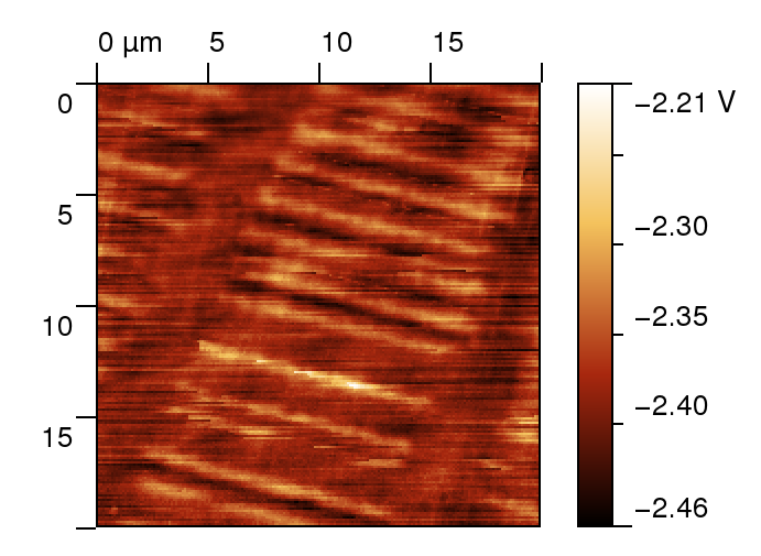 |
| MFM image of bits on a harddisc plate |
Regarding the electric and magnetic fiels characteriation, in our department we are active especially in the calculation of the
electrostatic field distribution between the probe and the sample and we deal with problems related to the resolution of techniques such as KPFM.
For these purposes we use the Finite Element Method or alternatively the Finite Difference Method in combination with FDTD method.
|

